PCAP touch screen customizations – definitions, capabilities and applications


Estimated reading time: 10 minutes
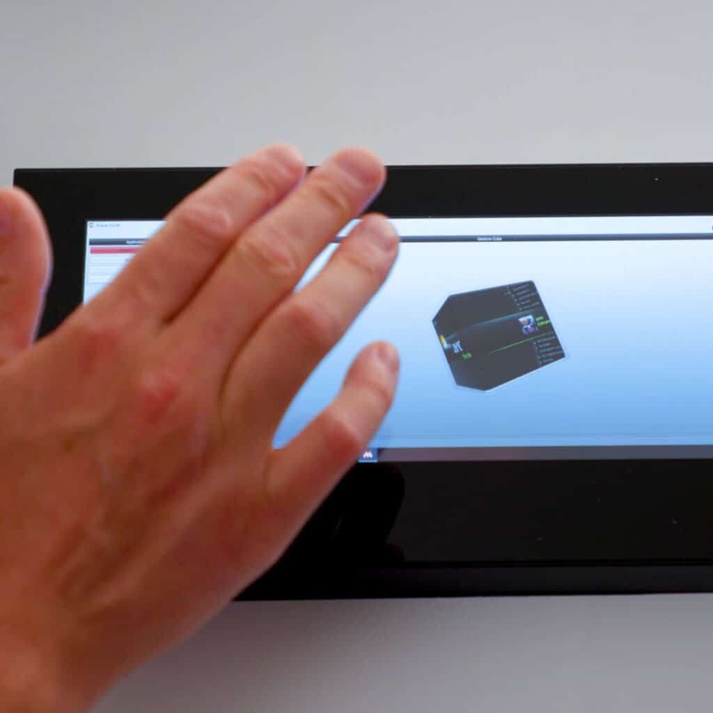
What is projected capacitive touch?
Projected capacitive (PCAP) touch screens are the latest iteration of a long history of touch sensor technologies dating back decades. The usage of PCAP touch screens has risen in conjunction with the proliferation of consumer electronics, medical device advancements and more sophisticated automotive applications, creating breakthrough specializations and use cases.
A PCAP screen’s conductive grid picks up changes in capacitance, which is the mechanism behind registering a touch. Paired with different bonding techniques, surface treatments and touch controller tunings, the ability to customize PCAP touch screens has led to endless permutations of highly successful touch display products.
What’s the difference between PCAP and resistive touch?
PCAP technology differs from resistive touch screens.
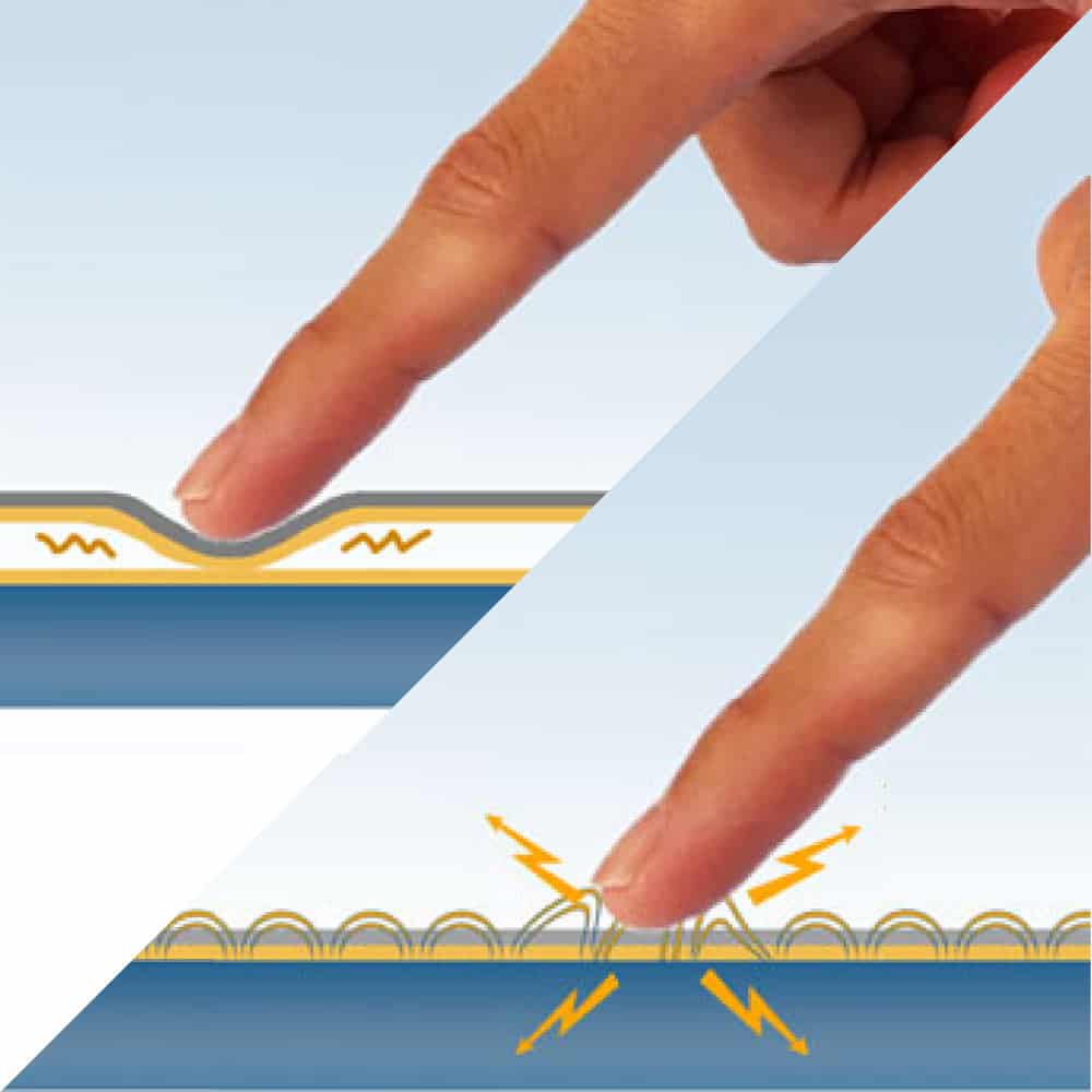
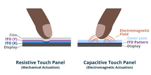
Resistive touch sensors register a touch when force is applied to the screen. When pressed against the screen, a finger creates an indent on a top film, which makes a connection with electrodes at the bottom of the stack. This change in resistance is how touch is recognized.
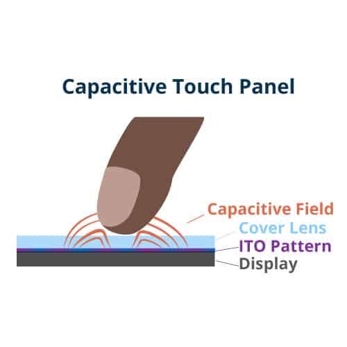
PCAP screens use two layers of electrodes (X and Y) that form a capacitive electromagnetic field around them. When a finger, stylus or other conductive object hovers or touches the screen, it results in an electric charge that enables the processing system to identify, register and respond to the signal. A finger, for example, penetrates the electromagnetic field, creating a change in capacitance.
PCAP sensors have almost completely replaced resistive touch sensors over the years due to their numerous advantages. They can support multi-touch, gestures and 3D proximity sensing, and provide superior reliability and durability. This makes them ideal for automotive, consumer, medical, and industrial applications that require more functionality than buttons and single points of contact can offer.
PCAP tunings and customizations
PCAP technology is highly customizable and can be designed to individual customer needs. Engineers can tune PCAP touch sensors for application-specific sensitivity and accuracy, using custom touch controller algorithms. These capabilities make PCAP touch sensors an ideal solution for applications with rigorous requirements.
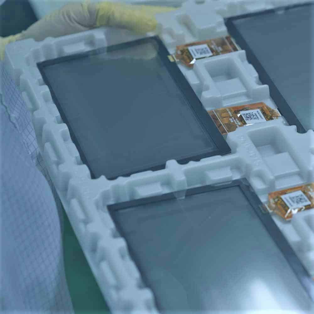
New Vision Display has decades of experience engineering high performance standards into integrated display products. Backed by its renowned PRECI-Touch® sensors, NVD is a leading designer of PCAP touch screen solutions for some of the world’s largest original equipment manufacturers (OEMs).
PCAP stack-ups and substrates
Touch sensors can be designed using various substrates and stack-ups based on the customer’s environment needs. Some of the stack-ups NVD can support include:
SITO (Single-layer ITO)
SITO touch sensor stacks have a single ITO layer with the X-Y pattern, usually a diamond pattern, on the top surface of the substrate (glass or film). The patterning has cross bridges, made of ITO or metal, that allow the X and Y electrodes to cross. They can be further customized with a glass lens with optional back printing, optically bonded to the sensor. This design eliminates the second layer of ITO present in DITO touch panel stacks and reduces the channel-routing margin outside the active area.
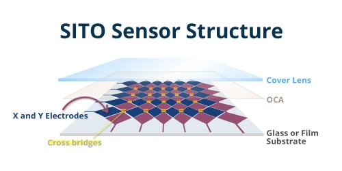
This is one of the most effective PCAP stack-ups, as it offers a high degree of accuracy as well as more control of charge time and sensitivity. SITO touch panels are the preferred solution for instrument clusters in automobiles, yacht navigation controls, and other applications requiring high sensitivity and control. They are also more accurate for rugged environments, water and salt-water immunity, and use with glove or stylus.
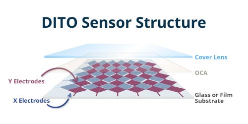
DITO (Dual-layer ITO)
DITO touch panel stacks have ITO layers on both sides of a glass or film substrate, with Y-patterning on the top sensing surface, and X patterning is on the bottom surface. DITO sensors are customizable with a glass lens with optional back printing, optically bonded to the sensor. They are a low-cost solution, which provides high resolution and accuracy.
OGS (One Glass Solution)
OGS stack-ups are newer to the market. The cover lens and the entirety of the touch stack-up itself are contained within one piece of glass, with all patterning completed on the back surface of the cover lens.
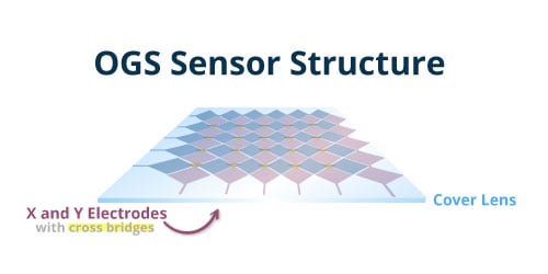
OGS is not often recommended for many industries, since the ruggedness of the stack is concentrated on the one and only piece of glass, increasing the chance of breakage. Additional layers, while adding mass to a stack-up, also help to make those options more durable. However, the slimmer and lighter construction can be attractive to customers and useful in certain (small-sized) applications. Also, the manufacturing costs are lower because of the reduced processing and fewer materials required.
2-layer film
A 2-layer film touch sensor stack has X and Y electrodes patterned on two different film layers, bonded together using OCA. The Y electrodes are patterned on the top film layer, and the X electrodes are patterned on the bottom film layer. This stack is customizable with additional protective cover lens optically bonded to the sensor, with optional back printing.

This option is often used in situations where cost is a critical factor, as film-based stack-ups are less expensive than those incorporating glass. It’s also useful in curved touch applications. However, applications where users might be expected to wear polarized sunglasses should be avoided, due to the birefringence characteristics of PET films.
2-layer glass
A 2-layer glass touch panel stack has X and Y electrodes patterned on two different glass layers, bonded together using OCA. The Y electrodes are patterned on the top glass layer, and the X electrodes are patterned on the bottom glass layer. This stack is customizable with additional protective cover lens optically bonded to the sensor, with optional back printing. This was the initial structure used for PCAP stack-ups.
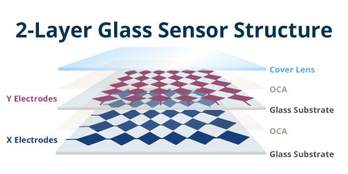
The high number of processes and materials involved in manufacturing this type of touch screen increases the rate of failure compared to other options, introduces more opportunities for external cosmetic defects, and increases the thickness and weight of the touch panel. Manufacturers have largely moved on to thinner and more efficient touch screen structures with better reliability and fewer manufacturing processes.
ITO patterns
The most evolved ITO pattern is diamond-shaped pattern. Whether the pattern is two-layered or co-planar with cross bridges is dependent upon the stack-up used.
- 2-layer patterns:
- DITO stack-ups have X and Y patterns on opposite sides of the same glass or film substrate
- 2-layer glass/film stack-ups have X and Y patterns on two separate layers of glass or film.
- Co-planar with cross bridges:
- SITO or OGS stack-ups use a co-planar pattern with cross bridges.
The diamond-shaped pattern provides an excellent user experience, supporting multi-touch functionality as well as use with stylus and gloves.
Chip mountings
One final point of differentiation among PCAP touch panel designs is how and where the chip is mounted. Two methods can be used:
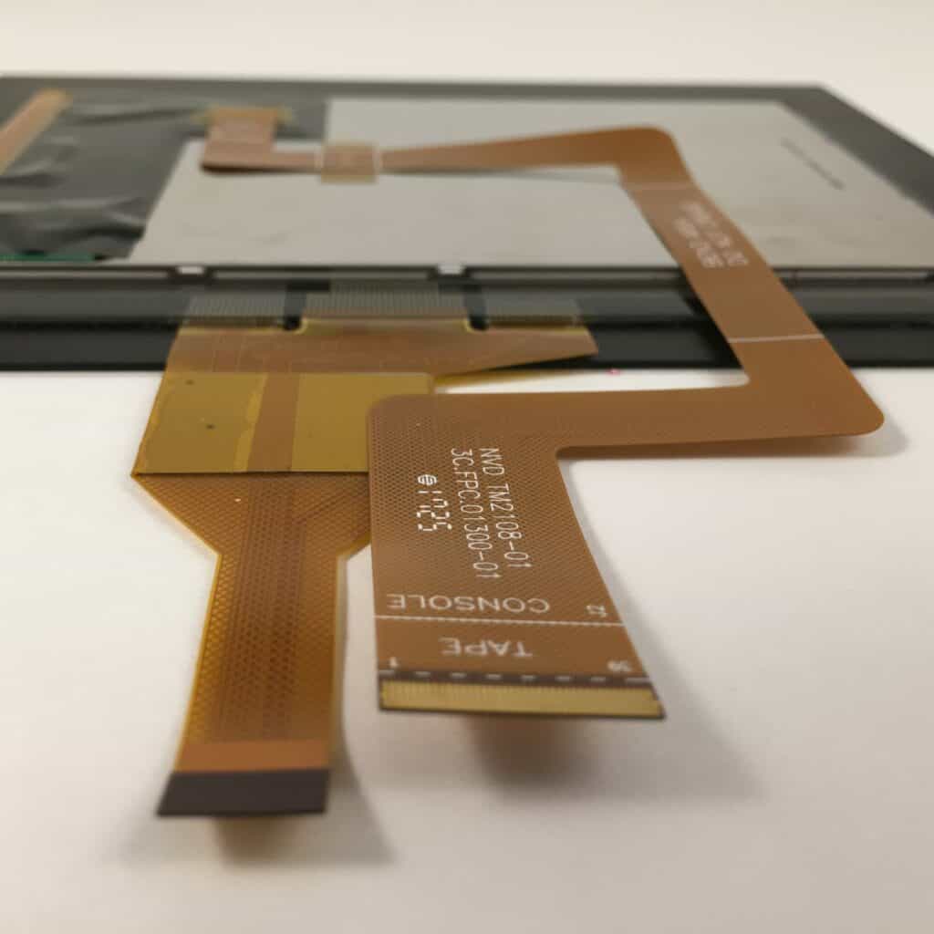
- COF (Chip-on-flex:) The controller and supporting electronics are on a flexible substrate. This is the primary chip integration method used for touch sensors due to it being slim and flexible, but may not be possible for sensors larger than 15 inches.
- COB (Chip-on-board): The controller and supporting electronics are integrated on a printed circuit board (PCB). Chip-on-board is typically used for sizes above 15 inches or if a customer prefers their touch electronics to be hosted on their own board.
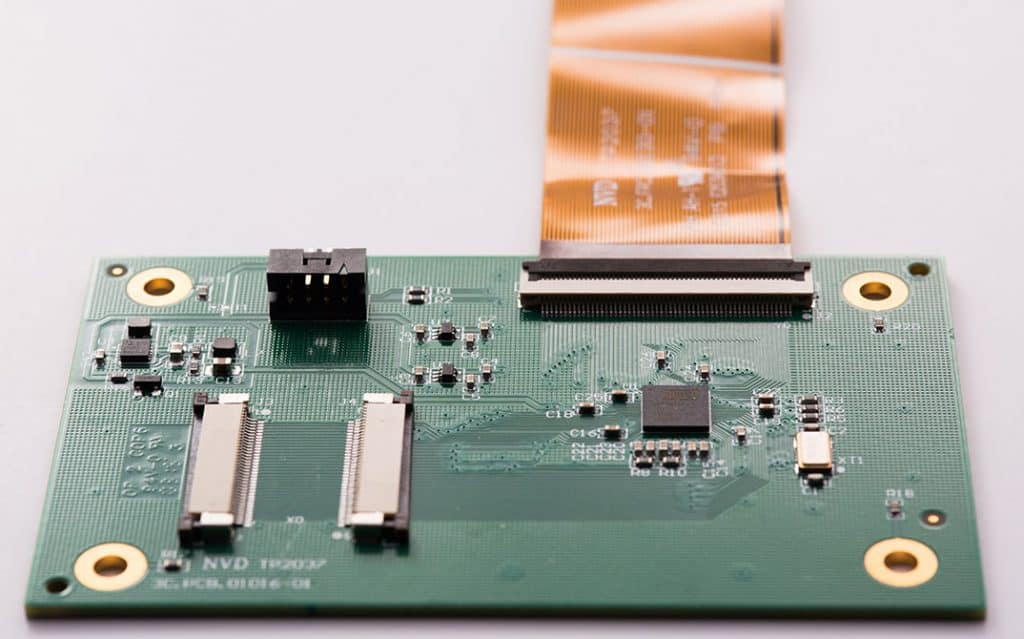
Chip-on-Board 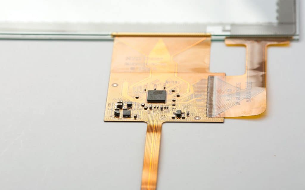
Chip-on-Flex
Bonding methods
Touch, display, and cover lens components can be bonded together in a number of ways:
Bonding of touch sensor and display:
- Optical bonding: Using an optically clear adhesive (OCA) or liquid glue to bond the touch and display components together, called optical bonding, is the optimal solution for many applications. In an optical bonding stack, air gaps are eliminated, creating a moisture and dust barrier and near-perfect optical transmission with low reflectance. This process also offers greater resistance to impacts, meaning greater overall durability.
- Air gap bonding: Another option for touch and display bonding is to use a double-sided tape around the perimeter of the display. Though lower in cost than optical bonding methods, this solution has lower optical performance, higher chance of dust and moisture penetration, and reduced shock and vibration resistance. There are ways to reduce system reflectance within an air bonded module by using anti-reflective (AR) films or coatings on the air gap surfaces and/or applying display polarizers.
Optical bonding of touch sensor and cover lens:
- Optical bonding: Touch sensor and cover lens components are always bonded together using an OCA film or liquid glue. Currently, air gap is not used to bond the two layers together because the air gap can cause uneven touch sensitivity on the surface. Optical bonding also provides near-perfect optical transmittance with reduced reflection.
Looking for guidance? Give us a call.
NVD is one of the most trusted PCAP touch sensor manufacturers with decades of experience serving major OEMs across all markets. Our PRECI-Touch® solutions are known for their performance in some of the most challenging applications and can be customized to your unique application requirements. We also provide full integration with custom LCD/OLED displays, cover lenses, and peripherals.
For more information on our PCAP technology capabilities, or to discuss your project with our experienced sales and engineering staff, contact New Vision Display today.
Our experienced sales team can recommend the right touch panel for your use case.